Guidelines for EMC design
Designers of electronics products can do a number of things to prevent users from having a bad experience with the product in use.
Malfunctions due to electrical issues
When a product stops working, it is irrelevant whether it happens due to the environment of use such as temperature, humidity, mechanical breakdown or too poor EMC properties. The user simply experiences that the product no longer works as intended. Maybe it needs to be turned off and on again. Or maybe it can be done by exiting a menu in the control panel and then re-entering. Maybe the product is defective and needs to be replaced with a new one. Whatever the reason, the user has had a bad experience with the product, which the designer can make an effort to avoid.
Different efforts depending on level
Fortunately, there is a large range of design tools that the electronics designer can use. Optimising the design can be divided into several levels (see figure 1), so that the user - who typically only experiences the ‘system’ level - is guaranteed the best possible functionality.
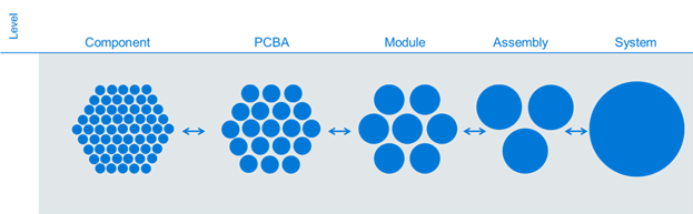
The research project PPEPP (Proactive Paradigm for Electronic Product Reliability), led by FORCE Technology, operates with scalability of design efforts depending on whether work is done at the printed circuit board (PCBA) level or on the cabinet of a product. If high tolerance for electrical disturbances is to be designed, then design activities at all levels may have to be undertaken at the same time.
The important PCB
Years ago, the metal cabinet was an important part of the EMC design. In modern designs, there is often no cabinet, and the EMC design activities have to be at the module, circuit board (PCBA) and component level. The board must be able to withstand electrical interference from radio transmitters (mobile telephones, NFC, WiFi) and electrostatic discharges (ESD) in daily use without any form of shielding. It puts pressure on the choice of components, design of printed circuit boards and especially attention to the interface between different parts (or printed circuit boards) in the same device.
Briefly summarized
All in all, EMC considerations can be concentrated on a few crucial factors:
- The printed circuit board is central. A printed circuit board without at least one 'comprehensive' ground plane (and preferably also some supply plans) can hardly achieve the desired EMC properties. Four layers in the print is usually the minimum. Two layers require great care! Also, pay attention to keep the impedance level in all sub-circuits 'low' (i.e. preferably not MΩ-size resistors).
- The power supply forms the bulwark and the protection between the printed circuit board and the mains. Overvoltages can occur in kV magnitude and covering a frequency range from kHz to hundreds of MHz.
- If the product consists of more than one printed circuit board, focus should be on the wiring interface between the parts. Signal filters and surge protection are effective protection against both signal interference and communication and at the same time reduce the noise that may be generated by the printed circuit board itself.
Read more
If you would like an elaboration of the EMC design guidelines from the PPEPP project, you can find further information in this document:
forcetechnology.com/EMCGuidelines.
This article was published in SPM Magasin, marts 2020.