Detecting moisture levels in circuit boards using MLI
A moisture level indicator (MLI) measures the saturation in a section of a printed circuit board (PCB). The indicator brings you one step closer to the truth about the moisture content of your PCBs.
The MLI was developed as part of Long Live Products and Materials, a project FORCE Technology is conducting for the Danish Agency for Higher Education and Science. The project's fundamental focus is on ensuring the availability of sustainable products with long, known lifetimes. Being aware of a product's health, or its state at a given point in time, is important to achieve this. Moisture content in printed circuit boards is a particularly interesting parameter to investigate here.
Excessive moisture in a PCB can cause problems during manufacturing using typical wave and reflow soldering processes, such as delamination, blistering, solder pad lifting, cracks between board layers etc. For these reasons, board manufacturers specify drying processes (e.g., oven drying) to be performed before soldering if a board is suspected to contain moisture.
However, this project focuses primarily on issues that occur in PCBs during use. These include:
- excessive leakage currents and short circuits
- corrosion (migration and corrosion of traces/platings)
- disconnections.
How does MLI work?
In short, the MLI measures the electrical capacitance (in farads) of a section of a multilayer PCB. The method is the same as that used for a commercial capacitive humidity sensor. It consists of a hygroscopic material (a dielectric) placed between two electrodes, forming a capacitor. The dielectric is typically a polymer, such as polyimide. The upper electrode is perforated to allow humid air to pass through it and down to the dielectric.
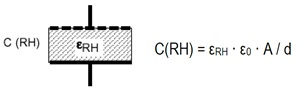
The sensor's capacity as a function of relative humidity, C(RH), is given by:
ɛRH is the relative permittivity (or dielectric constant) for the polymer at a given relative humidity, ɛ0 is the vacuum permittivity, A is the electrode area (the "shared" area between the two electrodes), and d is the distance between the electrodes.
In the MLI, the dielectric is a section of the board itself, which consists of epoxy (e.g., FR4). The electrodes are the copper layers, one of which must be sufficiently perforated (i.e., sufficiently free of copper) to allow humidity entering the epoxy, but not so much that the shared electrode area (A) is too small. For dry epoxy, ɛR is about 4.5. For pure water, it is about 80 (at room temperature). Because of this, despite epoxy's low maximum moisture uptake (about 0.8–1.2%), a change in capacitance of about 7–11% is still possible.
A "standard" PCB is typically 1.6 mm thick. An MLI for a two-layer PCB would give around 3 pF/cm2; that is, a very low capacitance. At this scale, a 7–11% change would be very difficult to measure unless the measurement area was very large (in practice, the entire PCB). In addition, moisture diffusion through epoxy is slow and inversely proportional to the square of the penetration depth d. Consequently, it would take weeks for measurable changes to occur.
Advantages of multilayer PCBs
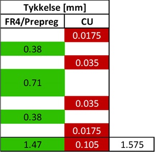
However, new opportunities arise when we consider multilayer PCBs (e.g. four layers). As shown in figure 2, a typical four-layer PCB comprises three layers of FR4 epoxy/prepreg and four layers of copper. The two outermost epoxy layers have a thickness of just 0.38 mm, making it possible to obtain approximately four times the capacitance per cm2 of board area, and approximately 16 times faster diffusion of moisture into the board. A greater number of capacitors per cm2 is now also possible, and these can be connected in parallel. If we additionally drill many small holes into the board in various places, response times of less than 24 hours (at room temperature) become possible. In most cases, this is sufficient to detect potential fault conditions associated with moisture penetrating into the board.
Practical measurements of MLI - methods and results
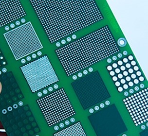
In this project, measurements were taken for four PCBs (10 × 16 cm). The boards were four-layer boards of the kind described above. Each board was prepared with 21 MLIs to test different combinations of size, placement (on both "raw" and individual boards), number of holes, and available copper area.
We chose this more "practical" approach since an analytic method for finding the optimal solution would be overwhelming and highly time-consuming, given the number of variables.
The combined (parallel) capacitance of the two outer layers was measured for each MLI.
The capacitance measurements were performed using a handheld Keysight U1733C LCR meter (priced at about 3500 DKK). However, a suitable board interface circuit (for a microcontroller, etc.) could likely be made inexpensively.
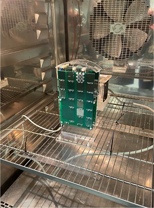
The four PCBs were tested pairwise at two different conditions: 25°C / > 90% RH (five weeks) and 65°C / > 90% RH (four weeks).
Figure 3 shows the curve for the MLI with the best performance at 25°C / 95% RH.
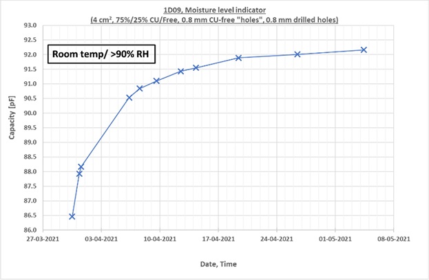
The curve in fig. 3 shows the results for the best MLI, which measures 4 cm2 and has a copper / empty space ratio of 75%/25% (196 holes with a diameter of 0.8 mm). The results confirm that measurable changes in capacitance can be obtained within a few hours. As expected, the total change in capacitance was of about 7%. These results also show that, depending on the application in question, MLIs may be optimised for either response time or change in capacitance (sensitivity). Furthermore, suitable measurement electronics could also detect and provide an indication of the development of condensation.
An MLI can naturally be built into a product's electronics (its PCB).
Applications of MLI
There are many possibilities for MLIs. All products used outdoors and in coastal/maritime environments are immediate candidates for use. Because MLIs can be integrated into a PCB, moulded applications are another ideal candidate.
The next tasks in this project are as follows:
- designing a suitable interface circuit
- verifying the overall design
- obtaining field measurements from practically integrated MLIs in products offered by manufacturers.

Compliance & Product Testing
Project