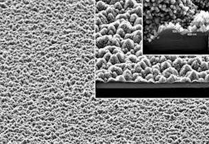
Surface characterisation
We provide comprehensive material analysis using advanced techniques, helping you identify issues and find effective solutions.
Testing and analysis of surfaces, structures, fractures, particles, impurities etc.
Experienced specialists using advanced equipment identify and solve your problems
We have advanced analysis equipment at our disposal and specialists within almost all material categories. This allows us to characterise your material and give you fast and reliable results.
We help you identify problems and solutions, whether it is for an R&D project, quality control or root cause analysis.
We have expertise in and access to techniques and equipment, ranging from relatively simple light microscopes to electron microscopes and advanced X-ray and neutron analysis tools.
Surface characterization methods and equipment
-
3D X-ray tomography
Characterization of materials using 3D X-ray microscopy
High resolution 3D X-ray microscopy and computed tomography are used to characterize the properties and behaviours of materials in a non-destructively manner.
By using a 3D X-ray microscope, it is possible to reveal details of microstructures in three dimensions (3D) and develop and confirm models or visualize structural details so the material in question can be thoroughly examined.
In order to achieve the highest contrast and submicron resolution imaging even for relatively large samples we recommend a 3D X-ray microscope.
Our X-ray equipment covers a range of different options with respect to:
- sample dimensions
- resolutions
- energies – for optimising contrast and/or penetration through various material types
- sample mounts, including environments for in situ investigations
Available instruments
- ZEISS XRadia 410 Versa
Xradia Versa architecture uses a two-stage magnification technique to enable you to uniquely achieve resolution at a distance (RaaD). Enlarge sample images through geometric magnification as with conventional micro-CT. In the second stage, a scintillator converts X-rays to visible light, which is then optically magnified. Reducing dependence upon geometric magnification enables Xradia Versa instruments to maintain submicron resolution at large working distances. This enables us to study the widest range of sample sizes effectively, including within in situ chambers.
- Nikon XT H 225
This instrument can penetrate larger and/or heavier specimens because of the higher energies available (up to 225 keV). The maximum field of view is 35 cm corresponding to a resolution of 200 µm, while the best achievable resolution is around 5 µm for mm-sized samples. Owing to the superior power (up to 225 W) the Nikon XT H 225 offers significantly faster imaging than the ZEISS Xradia 410 Versa for sample sizes between 5 mm and 5 cm at a comparable resolution.
- Xradia nanoXCT-100
This instrument is equipped with an Excillum MetalJet source. It is currently being commissioned for 3D imaging with a resolution down to 50 nm in samples up to 65 µm. The Excillum MetalJet operates at the Ga K-edge of 9.2 keV, thus at a higher energy (for better penetration) and with a larger flux (for faster imaging) compared to the standard Xradia nanoXCT-100 source (7.8 keV Cu rotating anode).
-
Optical 3D surface topography
For optical roughness measurement of surfaces, a special 3D microscope with high accuracy makes a “print” of the surface by using a vertical scan of the surface.
The roughness of a surface is essential for many surface characteristics. It defines how well a paint sticks or how much it wears on other surfaces in contact.
An example could be: Does the surface act as a catalyst or what friction is due to liquid fluids?
On surfaces with lubrication, roughness measurement can e.g. be used to measure how much lubricant the roughness can hold and how large the support is.
Many surface specifications have direct requirements for a maximum roughness expressed by one or more roughness parameters.
Therefore, it is also important what exactly we talk about when putting numbers on the rough. This is described in an international standard called ISO 4297: 1997, which describes a number of parameters, all of which are defined by measuring a height profile measured on a line on the surface.
Traditionally, such a profile is measured with an instrument with a diamond tip pickup with a well-defined rounding radius, which runs in a line above the surface and records the profile.
Optical measurement
For optical roughness measurement, a special 3D microscope with high accuracy makes a “print” of the surface by using a vertical scan of the surface. This method has a precision to 1 nm.
The method measures not only a line but an entire area, and not least, the measurement is made completely without physical contact with the surface. Therefore, one can measure on fragile surfaces, such as paper, textiles, plastics and other surfaces where a diamond in direct contact will be able to scratch the surface and thereby destroy it.
The method also makes it possible to measure roughness on curved surfaces with even very small radii of curvature. If you want to measure in hard-to-reach places, you can cast the surface with a special 2 component silicone rubber, which can then be examined in the microscope.
The area measurement also opens for new possibilities for measuring parameters that are not dependent on direction. A surface structure with a dominant direction (texture) can also be investigated with this method.
What does one get with a standard measurement?
For an optical roughness measurement at FORCE Technology, a roughness measurement according to ISO 4287: 1997 is carried out which includes all lines in the 3D image with the corresponding statistical uncertainty calculation. The parameters Ra, Rq and Rz are calculated.
In addition, the surface-based roughness parameters Sa, Sq and Sz are calculated. Other parameters from ISO 4287: 1997 can be calculated if desired and a definition of which parameters may be of interest to the customer can also be performed by our surface characterization experts. 3D images of the surface can also be provided.
-
X-ray crystallography
The method reveals the structure and function of many biological molecules, including vitamins, drugs, proteins and nucleic acids such as DNA. Using X-ray diffraction, one may determine the three-dimensional atomic structure in chemical compounds, materials and proteins.
X-Ray Crystallography uses the uniformity of light diffraction of crystals to determine the structure of a molecule or atom. Then they use an X-ray beam to “hit” the crystallized molecule. The electrons surrounding the molecule diffract as the X-rays hit them. This forms a pattern is called the X-ray diffraction pattern.
The 3-dimensional atomic structure is the basis for understanding for example material behavior or reaction mechanisms in enzymes. The combination of crystallography with other methods is the key to understand, improve and manipulate materials.
Three different powder X-ray diffractometers are available.
- A fixed-stage STOE diffractometer with a curved IP-detector and a Cu source can be used for fast phase-identification of powder samples.
- For more detailed and/or specialised studies a pair of Rigaku SmartLab diffractometers are available for powders as well as bulk samples. These very versatile and high-resolution diffractometers use high-intensity rotating anode X-ray sources (Cu and Co respectively).
- Specific sample environments are available allowing for a wide range of experiments to be performed including e.g. raster scanning and temperature studies in the range 12-1000 K.
x-ray crystallography
A number of single crystal diffractometers are also available including an Oxford Diffraction Supernova instrument equipped with a four-circle kappa goniometer, an Atlas charge-coupled device detector, a Mo microfocus X-ray source, and an Oxford Cryosystems Cryostream device enabling temperatures in the range 100-450 K. Furthermore, Cu and Ag silver X-ray sources are available and the setups can fit diamond anvil cells for high-pressure experiments.
Total scattering experiments are carried out at synchrotron facilities around the world. Total scattering and pair distribution function (PDF) analysis enable studies of defects and deviations from the average crystal structure, containing both crystalline and amorphous phases.
-
Widefield microscopy
Get help within specific applications in R&D, quality assurance, and materials testing.
Light microscopy
Whether you aim for fundamental understanding in materials science or want to improve the composition of future materials for energy storage or metals lightweight construction, light microscopy will provide you data you need.
Inverted microscope for materials testing
Materials testing and quality control has never been easier. We can help you undergo specific applications in R&D, quality assurance, and materials testing.
-
Stereo microscopy
The stereo microscope can be used for a variety of different purposes like evaluation of surfaces or inspection of scratches on metal.
The history of the stereo microscope
The basic idea behind a stereoscopic microscope is simple. It was formulated in 1896 by the biologist Horatio S. Greenough, who wanted to see small biologic samples magnified, but with the same quality as with unaided eyes. In other words: in three dimensions and with all the depth information he needed to understand the irregular shape of his specimen intuitively.
He reckoned, one could build a microscope with two separate beam paths facing the object from two directions - exactly as human eyes do when observing a small object at a distance of 250 mm
The brain would fuse the two images together and produce a spatial image of the object with a high degree of depth perception. This thinking led to the first factory-produced stereo microscope.
ZEISS Stemi 508 stereo microscope
- ZEISS Stemi 508's apochromatic zoom optics and efficient stray light suppression give you a crisp three-dimensional image, distortion-free, without color fringes.
- Visualize objects in fields of view up to 122 mm.The large 8:1 zoom lets you observe even minute structures in high contrast.
- Use interchangeable apochromatic front optics and eyepieces to reach any magnification between 2× and 250×. Double your resolution or enjoy large working distances up to 287 mm without compromising optical quality.
- The CL4500 LED fiber optic cold light source delivers daylight quality, especially optimal for color critical applications. To receive special illumination contrasts choose ringlights for shadow-free bright- or darkfield illumination, single and dual spots for distinct shadow effects, line light for grazing light, diffuse illuminations for avoiding hotspots, or use polarization equipment to eliminate reflections.
-
Scanning electronic microscope
Electron microscopy is a versatile tool with a range of methodologies to characterize the microstructural features of a sample from 100pm to 100μm length scales.
The SEM scans the surface of the sample with a high-energy electron beam. When the incident beam of electrons hits the specimen, X-rays and three types of electrons are emitted: backscattered (or primary) electrons, secondary electrons, and Auger electrons.
SEM makes use of the primary, or backscattered, and the secondary electrons. High-resolution images are produced by SEM revealing details of around 1–5 nm using the secondary electrons. For identifying elemental compositions, characteristic X-rays are used by a technique known as EDX. The backscattered electrons are also used to form the image in this technique.
- ZEISS EVO 25 electron microscope
EVO 25 is the industrial workhorse solution with enough space to accommodate even the largest parts and assemblies.
EVO excels at extracting the maximum data quality from uncoated and unaltered samples. EVO also safeguards data quality on hydrated and heavily contaminated samples, by allowing these samples to remain in their native state. Additionally, the LaB6 emitter will give that extra bit of resolution, contrast and signal-to-noise that is important when imaging and microanalysis get challenging. EVO 25 has a stage that can handle weights up to 2 kg even with tilt. Additionally, the large chamber will accommodate multiple analytical detectors for the most demanding microanalysis applications.
- Electron Microscope Analyzers
Our electron microscopes are equipped with a unique range of analysis methods for materials characterization on electron microscopes: EDS, WDS, EBSD and Micro-XRF.
- X-Ray Fluorescence (XRF)
This technique uses an X-ray source that is angled at the coated substrate and the solid state energy dispersion sensor is arranged at the complimentary angle to collect the X-ray fluorescence (XRF). The X-rays cause electrons to be ejected followed by a movement of electrons into the electron vacancies resulting in an electron relaxation which is accompanied by an emission of X-rays known as X-ray fluorescence. These X-rays are material dependent and so the composition of compounds can be determined.
- Energy Dispersive X-Ray Spectroscopy (EDS)
Energy-dispersive X-ray spectroscopy (EDX) is used to analyse the elemental composition of solid surfaces. X-ray emission is stimulated by the irradiation of the surface with a high energy beam of charged particles or a focused X-ray beam. Excitation of the electronic structure of an atom can produce an X-ray emission, the energy signature of which is a unique characteristic of each element. Therefore a “fingerprint” or “signature” spectrum can be obtained allowing element identification via comparison with reference spectra.
- Electron Backscatter Diffraction (EBSD)
The data collected with EBSD is spatially distributed and is visualised in maps and images, and is powerful for looking at localised features or non homogeneous samples. It can be used to study specific grains, local texture changes and low volume phases. EBSD can provide good phase discrimination, and when used in conjunction with EDS (i.e. when the chemistry is also available) offers excellent phase identification.
- Wavelength Dispersive X-ray Spectroscopy (WDS)
The WDS spectrometer can acquire the high count rate of X-rays produced at high beam currents, because it measures a single wavelength at a time. This is important for trace element analysis.
- ZEISS EVO 25 electron microscope
-
SAXS - Small-angle X-ray scattering
SAXS is a universal technique applicable to a broad range of particle sizes, from small peptides to huge macromolecular machines with molecular weight from about 5 kDa up to 100 MDa.
With the brilliant synchrotron sources, robotic sample changers and novel approaches to reconstruct 3D models, SAXS became a major tool to rapidly and comprehensively characterize macromolecular and nanostructured systems.
The main principles of SAXS were developed in the late 1930s by A. Guinier with his studies of metallic alloys. Already in the first monograph on SAXS by Guinier and Fournet (1955) it was demonstrated that the method yields not just information on the sizes and shapes of particles but also on the internal structure of disordered and partially ordered systems.
Conceptually, a SAXS experiment is simple: a sample is illuminated by X-rays and the scatteried radiation is registered by a detector. As the SAXS measurements are done very close to the primary beam ("small angles"), the technique profits immensely from the brilliance of X-ray photon beams provided by particle accelerators known as synchrotrons.
SAXS laboratory equipment
For laboratory SAXS analysis, the SAXS instrument comprises a next-generation SAXS instrument using advanced networked instrument control and data analysis. The instrument is fully automated and remotely controllable with capability of performing SAXS, MAXS, WAXS, GISAXS and Reflectometry on both isotropic and oriented samples.
The SAXS instrument is used for structural studies of materials of various kinds, including polymer systems, platinum based membranes for fuel cells, gels for replacing human intraocular lens, butter and cheese, and bio-membranes and protein structure in solution.
Services

Nicole Ciacotich
ESS & MAX IV
The European Spallation Source (ESS) and MAX IV are two new large-scale facilities currently under construction in Lund, Sweden.
These two facilities will make the Oresund region a world leading area for material research in the coming years.
Application examples in Advanced Neutron and X-ray Science:
- Visualize hidden structures and defects by 3D Imaging with X-ray and neutron technologies
- Investigate nanostructures
- Detect trace elements and impurities
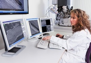
Advanced surface characterisation and analysis
Investigation and analysis of surfaces, structures, fractured surfaces, particles, impurities etc.
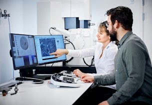
Identification of foreign bodies and contaminants
Foreign material can be a potential hazard in pharma and food production
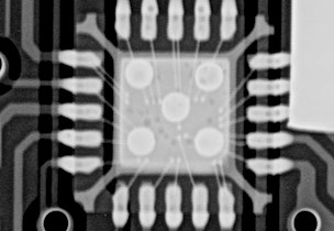
Digital X-ray inspection
Digital X-ray inspection of everything from laser welds and microchips to paintings.
Facility

